In semiconductor industry, it always requires active nanoscale device materials with high carrier (i.e. electron and hole) mobility similar to the fact that railway transport needs efficient high-speed trains. However, typical semiconductor materials, such as InP nanowires, usually have unavoidable crystal defects slowing down their electron mobility. This low electron mobility constrains the successful application of InP nanowires in high-performance field-effect transistors and photo-detectors, etc. Therefore, it is great challenge to minimize the crystal defects in order to “pave a flat and straight railway” for high-speed electron transport. In the literature, InP nanowires usually grow in the thermodynamically favorable orientations, such as <111> in cubic phase and <0001> in hexagonal phase. Since these two growth planes have similar atom alignments, a rotation of {111} plane atoms would easily change to {0001} plane atoms. Therefore, these nanowires usually have the inter-stacking atoms forming crystal faults, which limit their electron mobility < 1000 cm2/Vs. Recently, single-crystalline nonpolar-oriented InP nanowires can be successfully obtained with the minimized crystal defects and thus the high electron mobility, as demonstrated by the work collaborated among Prof. HAN Ning at Institute of Process Engineering, Chinese Academy of Sciences, Prof. YANG Zaixing at Shandong University, Prof. Johnny C. Ho at City University of Hong Kong, Prof. WU Xinglong and Prof. LIU Lizhe at Nanjing University. In this work, the obtained InP nanowires are uniquely stacked along the {2110} crystal planes. In this plane, the atoms are strongly inter-bonded to the three nearest planes, prohibiting the possible rotation of the plane atoms. Importantly, there are limited stacking faults so that the electrons can exhibit a high mobility of 2000 cm2/Vs, approaching the theoretical limit. Due to the high electron mobility, a low subthreshold slope of down to 91 mV/dec is obtained for the fabricated transistors and a high photoresponsivity of 104 A/W is obtained for the constructed photodetectors. Why these InP nanowires will grow in nonpolar orientation uniquely different from the others reported in the literature? The adopted Pd catalyst plays the key role here. The high melting point Pd will form a solid PdIn alloy for the InP nanowire growth. The preferred orientation of PdIn<210> will dictate the InP stacking planes of {2110}, which would be called the catalyst epitaxy. This research is published online in ACS Nano (Nonpolar-Oriented Wurtzite InP Nanowires with Electron Mobility Approaching the Theoretical Limit, https://pubs.acs.org/doi/10.1021/acsnano.8b05947) 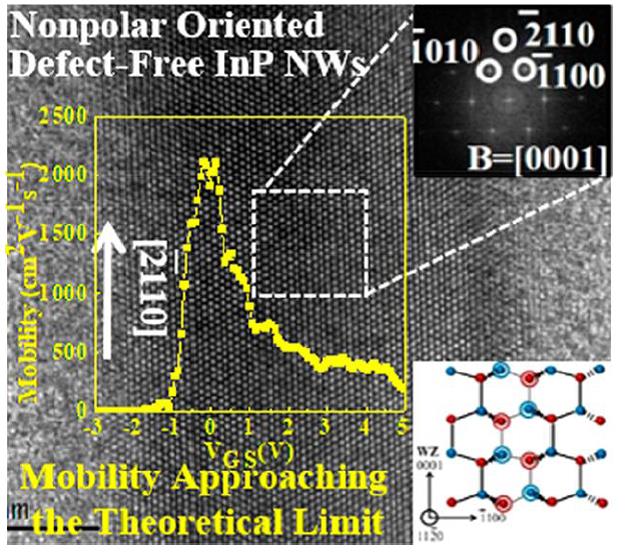 Catalyst epitaxy enables single-crystalline and high-electron-mobility InP nanowires (Image by HAN Ning) Media Contact:
LI Xiangyu
International Cooperation Office, Institute of Process Engineering, Chinese Academy of Sciences, Beijing 100190, P. R. China.
E-mail: xiangyuli@ipe.ac.cn
Tel: 86-10-62551358
|